Monday, December 22, 2014

Fast PWM on Arduino Leonardo

Today I will talk about PWM generation.
The Arduino boards provide pseudo analog outputs using the analogWrite( ) function. This function is not available on all pins, only the ones marked with the ~ symbol. The Analog Write function doesn't provide a real analog output but a PWM signal instead.

Arduino Leonardo Board
A PWM (Pulse Width Modulation) signal is a pulsed binary signal. As it is binary it can only have two output states "HIGH" and "LOW". The analog information is not on the signal levels but on the width of the generated pulses.We define Pulse Width as the width of the HIGH pulses and Duty Cycle, represented with a lower case delta letter, as the fraction of the Pulse Width to the total period T of the signal. The frequency of the PWM signal is defined as the inverse of the period.
PWM Signal

The mean value of the PWM signal depends on the Duty Cycle and the voltage values associated to the HIGH and LOW levels:
If the LOW level is zero, the the mean value of the PWM signal is:

That way, the mean value of the signal is proportional to the Duty Cycle.


Arduino analogWrite( ) function maps a 0 to 255 input value to a 0% to 100% Duty Cycle. As the HIGH level is about 5V and the LOW level is near to zero, the mean value of the signal generated using  analogWrite(pin,x) is:
 
If the device connected to the pin has lower bandwidth than the frequency of the PWM signal, it will work as low pass to the signal an only will see the mean value. Arduino Leonardo PWM pins use frequencies of  488Hz or 976Hz. When you use analogWrite on a LED, as LEDS have usually higher than 1kHz bandwidth, the LED will turn full ON and OFF as indicated on the PWM signal. Our eye, however, has a bandwidth (fusion frequency) up to about 100 Hz depending on the ambient ligh levels. As the LED pulses at a higher frequency than the eye bandwidth, we only see the mean value and seems that the LED lights at intermediate levels between ON and OFF.
The same applies if we use a PWM signal to drive a motor. Normal DC motors, due to their inertia, have bandwidths near or below the Arduino PWM frequency, so the motor works as if a constant variable voltage where applied. In fact, PWM operation at low frequency can make the motor work better at low speeds.

All in all, the 500Hz to 1kHz PWM frequency in stock Arduino is adequate to drive motors. If we want, however, to generate an audio signal, the analogWrite function does not work.The hearing bandwidth in humans is arround 20kHz, much higher than the Arduino PWM frequency. Typical speakers are usually designed inside the human hearing bandwith so applying a PWM signal to them will produce an audible tone at the PWM frequency.

One of the utilities to generate a high frequency PWM signal is going beyond the speaker and hearing bandwidths so that we can use an PWM signal to generate an audio signal.


Stock PWM on Arduino Leonardo

First we start explaining how the PWM is implementated on the Arduino Leonardo board. In most Arduino boards the PWM signals are generated using timers. Timer peripheras provide hardware PWM generation so that the CPU don't need to use any of it's execution resources to generate the signals. Each timer has a limited number of PWM signals than can be generated by hardware. 

The Arduino Leonardo, as the Micro and Esplora use the ATmega42u4 MCU. It includes four timers: Timer 0, Timer 1, Timer 3 and Timer 4. Timers 1 and 3 are equal, but the rest of timers are quite different. Other Arduino Boards make use of other timers provided by the MCUs they use.

The following table shows the timers usage to generate PWM on the Arduino Leonardo board. You can see it and more information on my Arduino Leonardo spreadsheet.

PWM Timers in Arduino Leonardo
Arduino uses the timers for other functionalities. For instance, Timer 0 is also used to record the pass of time as is needed for the functions millis( ), micros( ), delay( ) and delayMicroseconds( ). You don't wanna mess with Timer 0 operation as it will disturb all timing functions. 
Some Arduino libraries make also use of timers. The Servo library uses Timer 1 on the Leonardo while the MsTimer2 library uses Timer 4. You should know that using any library that needs a timer will affect any PWM pin associated to that timer.

There are several two basic ways to create a PWM signal using a timer.

Single Slope PWM

The timers are typically based on a Counter. The counter uses a clock input and, at each active clock edge, the counter changes state. One typical mode of operation for a timer involves increasing the counter at clock each clock edge until it reaches a maximum value. Once this value is reached, the counter returns to zero and the process repeats.That gives a sawtooth waveform on the counter values as is depicted in the figure below. One full cycle of the sawtooth will need Count Max + 1 clock cycles.

Single slope PWM

Timer peripherals usually include several capture/compare registers. In order to create a PWM signal, a compare register is linked to a hardware output of the MCU in a way that makes this output high if the counter is below or equal to the compare register value. That will give, for each compare register, a PWM signal whose duty cycle depends on the compare value. 
All PWM signals generated by the same timer, will have the same frequency as the start of the generated pulses will allways be at the falling edge of the sawtooth signal.
If we have several PWM signals regenerated with different compare registers at the same timer, all of them will have the rising edge at the same times.

The Arduino analogWrite( ) functions operate the ATmega 32u4 Timer 0 at single slope. The 250kHz clock used is obtained dividing by 64 the 16MHz system clock. The final PWM frequency will the be 976Hz.
Timer 0 has two compare channels A and B associated to two compare registers OCR0A and OCR0B. The two channels are linked to two hardware outputs OC0A and OC0B that are used as Arduino pins numbers 11 and 3.

Dual Slope PWM

Another way to generate a PWM signal configures the counter to increase at each clock edge, and when it reaches the maximum value, start decreasing one number each clock cycle until it reaches zero and the patter repeats again. That will give a triangle waveform instead of the sawtooth one.

Dual Slope PWM
We can also configure a capture register so that a generated output signal is high when the counter is below this register. This will generate a PWM signal as in the single slope case. The difference is that, if we have several compare registers, the PWM signal generated with each one will be synchronized at the center of the generated pulses.
This is handy in some kinds of motor control but the details are beyond this article.
In any case, the PWM frequency will be the same for all compare channels and will also be half of the value we would obtain if we used a Single Slope counter.


The Arduino analogWrite( ) functions operate the ATmega 32u4 MCU Timers 1, 3 and 4 in Dual Slope mode. A possible reason why Timer 0 is not operated also in Dual Slope can probably be due to the fact that Timer 0 is used to record the pass of time and, this use, is difficult to be implemented on a dual slope timer. Working on dual slope, all PWM pins associated to those pins use half the Timer 0 frequency working at 488Hz.
Timer 1 includes three compare channels A, B and C associated to compare registers OCR1A, OCR1B, OCR1C linked to hardware outputs OC1A, OC1B and OC1C. The Arduino software only uses the channels A and B that are related to Arduino pins 9 and 10. Channel C output OC1C is associated to the same 11 Arduino Pin driven by Timer 0. For whatever reason Arduino designers preferred to drive pin 11 using Timer 0 at single slope than use Timer 1 at dual slope.
Timer 3 only includes one hardware output OC3A at Arduino pin 5, associated to the compare register OCR3A.
Timer 4 is a special timer, but respect to PWM, it operates as Timers 1 and 3 in dual slope mode. It includes three hardware outputs OC4A, OC4B and OC4D associated to registers OCR4A, OCR4B and OCR4D. Only channels A and D are used in stock Arduino for pins 13 and 6. Channel B is associated to the same pin driven by OC1B so Timer 1, instead of Timer 4, is used for this pin.
All of that gives the table of the 7 PWM enabled Arduino Pins.


Fast PWM on Timer 1

If the maximum 976 Hz that stock Arduino analogWrite is not enough, we need to develop our own PWM functionality. Timer 1 is a good candidate as it has three available compare channels and don't mess with Arduino delay functions. You should take care if you use the Servo library because it also uses Timer 1.

Timer 1 is based arround a 16 bit counter. That means that it can count from 0 up to 65535 before overflowing. The timer has several modes of operations that include 12 PWM modes. The fastest PWM mode available is single slope 8 bits counting between 0 and 255. As single slope is faster that dual slope, it is also called Fast PWM mode.
You can also have 9 bits and 10 bits PWM modes with 511 and 1023 terminal counts that can operate on single and dual slope modes. Three bit modes 8, 9 and 10 for single and dual slope PWM gives a total of 6 PWM modes. The other 6 additional PWM modes use programmable terminal counts that can be any 16 bit value and is not restricted to 255, 511 or 1023.

The timer gets its clock from the global MCU prescaler that provides five frequencies from the system clock. The divide ratios are 1, 8, 64, 256 and 1024. That gives, using the 16MHz Arduino Leonardo system clock, the fiveclock and single slope frequencies shown below for standard 8, 9 and 19 bit modes:

Prescaler and PWM options
Using dual slope the maximum frequency will be half. We see that the maximum available PWM frequency on Timer 1 is 62.5kHz. That's enough to generate some sort of audio signal as it is beyond the audible range of frequencies.

In order to configure the timer we must program the Timer 1 registers TCCR1A and TCCR1B.


Bits 0, 1 and 2 of TCCR1B (CS10, CS11 and CS12) configure the clock options acording to the following table.


Bit 1 of TCCR1A (WGM11) and bits 3 and 4 of TCCR1B configure the waveform for the timer acording to the table:


Modes  1, 2, 3, 5, 6 and 7 correspond to the 6 standard PWM modes.

Once the timer is configured on one PWM mode, each of the three compare channels A, B and C can be enabled to generate a PWM signal. To do that, the COM1x0 an COM1x1 bits on register TCCR1A associated to a particular x channel (A, B, C) need to be configured according to the table:


The PWM value for each channel should be programmed in each channel compare register OCR1A, OCR1B and OCR1C.

All the above tables habe been taken from the ATmega32u4 datasheet.

Configuring the TCCR1A bits is not enough to generate the PWM signal at the output pins. We also need to configure them in output mode. From the ATmega32u4 we can see that the timer 1 outputs OC1A, OC1B and OC1C  are associated to port lines PB5, PB6 and PB7 (Arduino Pins 9, 10 and 11). We need to set those pins in output mode using the Port B Data Direction Register DDRB.


Fast PWM on Timer 4

Using Timers 0, 1 or 3  we can have up to 62,5kHz PWM signals, but the maximum possible PWM frequency is only available on Timer 4.
Timer 4 is a 10 bit timer that can operate at very fast speed due to its clock source options.
The ATmega32u4 MCU includes an USB peripheral. This peripheral needs a 48MHz clock frequency that goes beyond the maximum 16MHz system clock. In order to generate the USB frequency the MCU incorporates an internal PLL. In the Arduino Leonardo the PLL takes as input the 16MHz system clock and multiplies it by 6 to generate a 96MHz output frequency.
You don't want to mess with the PLL configuration on the Arduino Leonarda as it will break the USB communications. The only need you need to know about the PLL is that its output can source the Timer 4 peripheral.

The PLL register PLLFRQ includes among other things, two bits PLLTM0 and PLLTM1 that determine the input clock to Timer 4.


There are four options, don't use the PLL to source the timer (it will be sourced by system clock) or to use the PLL output divided by 1, 1.5 or 2. That will give 96MHz, 64MHz or 48MHz clock frequencies.


At the time of this writting the above table was missing from the official ATmega32u4 current datasheet. I needed to find an older datasheet to obtain the full PLL configuration register contents.

Timer 4 has an additional divider configured with bits CS40 to CS43 of the TCCR4B configuration register.

The available options are:


 That way, using the PLL and Timer 4 dividers you can have input frequencies betwen 96MHz and 5859Hz.

In a similar way than Timer 1, Timer 4 must select a waveform operation mode using bits WGM40 and WGM41 of the TCCR4D register.

The available options are:


Mode 00 is Single Slope while mode 01 is Dual Slope.

Observe that the PWM signal has a maximum count value defined in OCR4C register. As compare channel C register is used for the terminal count, there is no independent channel C PWM output.

PWM6 is an special PWM operation mode that uses all three available channels A, B and D to drive a motor. The details, that are beyond the scope of this document, can be found on the MCU datasheet.

After configuring the clock input, each channel x = A, B and D of Timer 4, can be configured with its own bits COM4x0, COM4x1 and PWM4x at registers TCCR4A and TCCR4C.
As we have explained channel C, used as terminal count, has no output unit so it cannot be used to generate PWM.

To operate one x channel in PWM mode you need to set to "1" the  corresponding PWM4x bit. After that, the COM4x0 and COM4x1 determine the mode of PWM operation. In the case of channel A in fast PWM mode we can choose:


Normal PWM operation corresponds to mode 10. Mode 11 will give a complementary output whereas mode 01 gives two complementary PWM outputs at different pins. The complementary signals can have some deadband between them so that one signal, and its complement are never active at the same time.
Similar tables can be found for channels B and D.

Fast PWM Test Code

I have put together all the above methods to generate PWM in a FastPWM Arduino sketch.


The sketch includes the needed code to operate 5 pins associated to Timers 1 and 4 in fast PWM modes.

Timer 1 Code

The code associated to timer 1 includes 4 functions and several defines. It can uses all three Timer 1 compare channels to generate PWM signals at Arduino pins 9, 10 and 11.

The pwm91011configure function must be called previously to the call of any other function associated to this timer. It configures the timer to operate in single slope fast PWM mode and sets the prescaler to the mode indicated on the function argument.
The five possible modes are  PWM62k,  PWM8k, PWM1k, PWM244 and PWM61 and are associated to the four available frequencies in single slope 8 bit PWM modes.

Functions pwmSet9, pwmSet10 and pwmSet11 configure the Timer 1 channels associated to pins 9, 10 and 11 to work in PWM mode and set the given PWM value (0 to 255).

After one of the three above functions is called, the PWM value can be fast changed using a direct access to the corresponding compare register. To ease the access, three definitions PWM9, PWM10 and PWM11 are associated to compare registers OCR1A, OCR1B and OCR1C.


Timer 4 Code
The code associated to timer 4 includes 3 functions and several defines also. It uses two of the three available compare channels A and D associted to Arduino pins 13 and 6. It doesn't use channel B because its Arduino pin 10 conflicts with the Timer 1 channel B previously used.
The pwm613configure function is similar to the one defined for Timer 1. It sets the PLL and PWM modes to properly configure Timer 4 in high speed mode from the 48MHz PLL tap and sets the terminal count in OCR4C to 8 bits (255). 
The input argument sets one of seven available prescaler frequencies for a 48MHz timer 4 clock input: PWM187k (187500 Hz), PWM94k  (93750 Hz), PWM47k  (46875 Hz), PWM23k  (23437 Hz), PWM12k  (11719 Hz), PWM6k   (5859 Hz) and  PWM3k  (2930 Hz). If you remenber the Timer4 options there where 15 clock prescaler options. The lower frequency ones are not implemented in the defines as they provide no advantage over stock analogWrite functionality.

Functions pwmSet13 and pwmSet6 configure the Timer 4 channels associated to pins 13, 6 to work in PWM mode and set the given PWM value (0 to 255).
In a similar way than timer 1, after one of the two above functions is called, the PWM value can be fast changed using a direct access to the corresponding compare register. Two definitions PWM13, and PWM6 are associated to compare registers OCR4A and OCR4D. An aditional PWM6_13_MAX definition has been added to access the OCR4C register that sets the PWM terminal count that is, by default, set to 255 (8 bits).


Setup and Loop Code

To check all the above functions Timer 1 is configured in setup to generate 62,5kHz PWM signals.  Timer 4 is configured for 187kHz. 4 signals are generated. At pins 11 and 13 11% and 75% fixed PWM values are set.  For pins 6 and 9, a variable 0% to 100% PWM value is programmed inside the loop function.
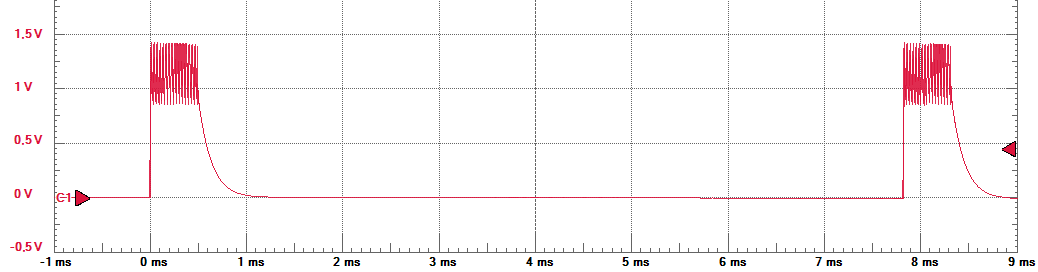
Generated Waveforms

The following figure shows the generated waveforms captured with the Logic Analizer of the Analog Discovery scope.


Timer 1 signals at pins 9 and 11 have the same risign edge as they are in single ramp PWM mode. The same applies to signals at pins 6 and 13 that depend on Timer 4. Signals at different timers are at different frequency so the rising edges don't usually coincide for both timer signals.

That's all for now. Timers are very usefull peripherals. PWM is only one of the timer applications. In the future I plan to talk also about generation of periodic events.


Code on Github (11/02/2018)

The code is now on Github:

https://github.com/R6500/Leonardo/blob/master/FastPWM.ino

Wednesday, December 10, 2014

Low level GPIO on Arduino Leonardo

The Arduino boards provide an easy entry in the microcontroller (MCU) world. With practically no knowledge on electronics and in no time yo can have a little project up and running.

The Arduino way to do coding builds over an extensive set of pre-coded libraries that hides the complexities of interfacing a MCU. That's all OK if don't need to go to the limits of what the MCU can do or if you don't mind to know about how the MCU does its things. But it you need to cut corners or if you want to learn about MCUs, you should try to depart a little from the Arduino way.

One good and bad thing about Arduinos is their uniformity. All arduinos use the same digitalWrite, digitalRead, analogRead and analogWrite functions. And they work the same, more or less, if you are using an Arduino UNO with an ATmega328 or an Arduino Galileo with an Intel Quark SoC X1000. But, as the MCUs used are different, they really don't work exactly the same.

If you want to go beyond the Arduino way, the uniformity falls off as the methods change depending on the MCU the board uses. If two boards use the same kind of MCU, the internal procedures will be similar, although not always equal. If two boards use a different MCU, the internal procedures can be quite different.

In this article I will target the Arduino Leonardo. This is a quite capable board that comes to substitute the old Arduino UNO. It includes an ATmega 32u4 MCU. This is part of the megaAVR familly of MCUs. Most classic arduino boards like the UNO (ATmega328), Mega 2560 (ATmega2560), Mini (ATmega168) are in this family. In fact, the Arduinos Micro and Esplora use the very same 32u4 MCU that uses the Leonardo.

Arduino Leonardo

The Arduino Leonardo don't need to use an additional chip to provide the USB communication because the MCU that includes can manage that itself. For the same reason, the board can emulate an USB peripheral like a mouse or a keyboard.

Using an Arduino to learn the insides of the ATmega 32u4 MCU has advantages and inconvenients. On one hand, the Arduino IDE provides all kinds of functions and libraries to do complex operations so you can do low level coding of only one part of the system. For instance you can leave the serial over USB communication to the Arduino libraries and do manual control of GPIO lines. On the other hand, the Arduino IDE tries to hide the low level sintax of the MCU and the bootloader method used to load the program don't provide any hardware debugging of your code.
To make things a little worse, the Arduino libraries make some use of the MCU internal resources and it's not always easy to know what libraries will you break if you take a step out of the Arduino way.

In this first article about the insides of the Arduino Leonardo I will talk about how the digital GPIO works. That is, I will talk about how to do low level operations equivalent, but faster, to the use of the pinMode, digitalRead and digitalWrite functions.


Arduino pins and Leonardo ports

The ATmega 32u4 MCU that powers the Arduino Leonardo features 5 digital GPIO (General Purpose Input/Output) ports. Each one is labeled with a leter, so we have ports B, C, D, E and F. 

Each port can have up to 8 digital lines (numbered from 0 to 7) associated with pins of the MCU package.

ATmega 32u4 pinout
As you can see in the above pinout, most package pins include references like PE6 (Line 6 of port E) and PB0 (Line 0 of port B). As the MCU package has 44 pins and as each of the 5 ports could have up to 8 lines, you can see that you could get out of pins if you include power supplies, Xtal and USB connections. I you obseve the pinout you will see, for instance, that there is no PD5 and that the port E includes only two lines. In fact, only ports B and D are complete (8 lines each).

The line distribution is:
  • Port B : 8 lines PB0 to PB7
  • Port C : 2 lines PC6 and PC7
  • Port D : 8 lines PD0 to PD7
  • Port E : 2 lines PE2 and PE6
  • Port F : 6 lines PF0, PF1 and PF4 to PF7
So you have 26 GPIO lines in total. You can also see this line distribution in the MCU internal block diagram description.

Internal ATmega 32u4 structure
The 26 GPIO lines are relabeled, in the Arduino functions, as lines 0 to 23. You can see that there are two lines missing. That's because PD5 and PE2 are not available as digital or analog lines in the Leonardo board. If you look at the board you will only see the numbers of 14 of the lines (0 to 13). The lines 14 to 17 are located on the male 6 pin ISP/SPI header and the lines 18 to 23 are alias names for the analog A0 to A5 lines that can also be used as digital I/O.

Top view of the Leonardo Board
The ATmega 32u4 features 12 analog inputs. That's more that the 6 A0 to A5 marked on the board. Those inputs are avalilable as the lines 4, 6, 8, 9, 10 and 12 and you can use the alias names A6, A7, A8, A9, A10 and A11 for those lines.

Why aren't all the extra analog lines marked as A6 to A11?
Well, because the original Arduino, with PDIP package, only had 6 lines and keeping the pin form factor of the board is important to provide board to board compatibility.
In other words, the Leonardo, with its 32u4 MCU is different from the UNO with its 328 MCU but the board is marked to use the same pin names.

Arduino UNO top view
The different port lines are not related to the standard Arduino pin names. That's because, to keep the board pinout compatibility, the lines that can give PWM signals using the analogWrite function need to be associated to lines 3, 5, 6, 9, 10, 11 and 13. 
In the UNO board the pin numbering is easy, digital pins 0 to 7 go to lines 0 to 7 of port D, lines 8 to 13 go to lines 0 to 5 of port B and analog lines 0 to 5 go to lines 0 to 5 of port C.
In the Leonardo, to keep things compatible, there is a mess of lines. Digital lines 0 and up are connected to PD2, PD3, PD1, PD0, PD4, PC6, PD7, PE6.... All messed up.

The only way to know with Arduino line relates to which port line on the Leonardo is using a written list as there is no logical distribution as it was on the Arduino UNO.

I you want to see which line goes with what, you can use the Arduino Leonardo Spreadsheet I wrote on Google Drive from the link below.


Bitwise variables and registers

Every digital port B, C, D, E and F has three related 8 bit registers. You can access those registers in a similar way that accessing byte variables. You only have to know their names. Every register has one pin associated to each port line. So, for instance, bit 3 (with weight 2^3 = 8), is related to the line 3 of the port. You can think of port registers as sets of 8 boolean values.

If you want to set bits 0, 4 and 6 of a 8 bit variable you can add its weights:

VARIABLE = 2^0 + 2^4 + 2^6;

That is:

VARIABLE = 1 + 16 + 64;

Or, in a more "C" style:

VARIABLE = 1 | (1 << 4) | (1 << 6);

To ease the naming of bits you can use the bit( ) macro that is defined in Arduino.h.
Using this macro you can use an easier bit assignment:

VARIABLE = bit(0) + bit(4) + bit(6);

To set one bit of a variable you can use the bitwise OR operator:

VARIABLE = VARIABLE | bit(3);   // Sets bit 3 of VARIABLE

To clear one bit of a variable you can use the bitwise AND and complement ~ operators.

VARIABLE = VARIABLE & (~bit(3));  // Clears bit 3 of VARIABLE

To ease clear and set of variable you can define two macros:

#define SET_FLAG(REGISTER,FLAG)     REGISTER|=(FLAG)
#define CLEAR_FLAG(REGISTER,FLAG)   REGISTER&=~(FLAG)

So, you can use:

SET_FLAG(VARIABLE,bit(3));   // Sets bit 3 of VARIABLE
CLEAR_FLAG(VARIABLE,bit(3);  // Clears bit 3 of VARIABLE

You can also set several bits at the same time:

SET_FLAG(VARIABLE,bit(2)|bit(3));   // Sets bits 2 and 3 of VARIABLE

CLEAR_FLAG(VARIABLE,bit(2)|bit(3)); // Clears bits 2 and 3 of VARIABLE


If you want, you can use the stock bitRead, bitSet, bitClear and bitWrite macros defined in Arduino.h:


It is important to know which are the Arduino macros as they are compliled in place and, because of that, they don't have the overhead associated to a function call.

Observe that, using the stock Arduino macros, you should not use the bit( ) macro in the calls:

if (bitRead(VARIABLE,3) 
       {
       // Do something if bit 3 of VARIABLE is set
       }
bitSet(VARIABLE,3);         // Sets bit 3 of VARIABLE
bitClear(VARIABLE,3);       // Clears bit 3 of VARIABLE
bitWrite(VARIABLE,3,value); // Sets or Clears bit 3 of 
                            // VARIABLE depending on value

Beware that you cannot use the bitSet and bitClear macros to set or clear several bits at the same time.


Low level digital I/O


The three registers associated to each port controls the port direction (similar to pinMode) the port output (similar to digitalWrite) and the port input (similar to digitalRead). Let's see the one by one.


Port Data Direction Registers (DDRB, DDRC, DDRD, DDRE, DDRF)

Those registers indicate, for each line, if it is an input or an output. Each bit on the register can only have two values:

  • "0" Indicates that the line is an input
  • "1" Indicates that the line is an output
So, for instance,  to set Arduino pins 10 and 11, associated to PB6 and PB7 in output mode you can write:

SET_FLAG(DDRB,bit(6)|bit(7));

This way, the above line is equivalent to:

pinMode(10,OUTPUT);
pinMode(11,OUTPUT);

But ocupies less program space and requires less time to execute.


Port Output Registers (PORTB, PORTC, PORTD, PORTE, PORTF)

When a port line is in output mode, as set with a DDRx register, this register holds the value that will be seen at the output line.
  • "0" Indicates a low value (next to 0 Volts)
  • "1" Indicates a high value (next to 5 Volts)
For instance:

SET_FLAG(PORTB,bit(6));

Is equivalent to:

digitalWrite(10,HIGH);

The low and high output values can be obtained from the datasheet of the ATmega 42u4.
DC Voltage Data
You can see that the low level output voltage Vol is guaranteed to be below 0.7V up to 10mA of sink current when the supply is 5V. In a similar way, you can see that the high level voltage is guaranteed to be over 4.2V up to 10mA of source current.


When a port line is in input mode, however, the PORTx register indicates if the port will feature or not a pull-up resistor.

  • "0" Indicates that no Pull-Up will be used
  • "1" Indicates that a Pull-Up will be used
It is important to note that when you configure one port from output to input mode, the previous value on the Port Output Register determine if it will feature or not a Pull-Up.

Pull-Up resistor data
As you can see from the data obtained from the MCU datasheet the Pull-Up resistors on the I/O ports are guaranteed to be between 20kOhm and 50kOhm.


That way:

CLEAR_FLAG(DDRB,bit(6));
CLEAR_FLAG(PORTB,bit(6));

Configures the Arduino pin 10, associated to PB6, in input mode.
And is equivalent to:

pinMode(10,INPUT); 

and

CLEAR_FLAG(DDRB,bit(6));
SET_FLAG(PORTB,bit(6));

Configures the Arduino pin 10, in input mode with a Pull-Up resistor to Vdd.
And is equivalent to:

pinMode(10,INPUT_PULLUP);


Port Input Registers (PINB, PINC, PIND, PINE, PINF)

This register always returns, when read, the logic state at the related port pin. This is independendent on the Input or Output configuration of the port.

This register is normally read for input pins to determine the state of the related lines, but it can also be read for output pins to verify that no external element is forcing a different logic state that the one we set.

Each bit reads:

  • "0" If the related line is at low level (Voltage below Vil_max)
  • "1" If the related line is at high level (Voltage above Vih_min)
For instance:

if (PINB&bit(6))  { // Do something 
                  };

Is equivalent to:

if (digitalRead(10)) { // Do something 
                     };
     

You can find the Vil_max and Vih_min thresholds in the table shown before from the ATmega 32u4 datasheet. As you can see they are:

  • Vil max = 0,2Vcc - 0,1V =  0.9V at Vcc = 5V
  • Voh min = 0,2Vcc + 0,9V = 1.9V at Vcc = 5V
Writing to the PINx registers have not relation with reading them. In fact, writing to a PINx register bit to "1" affects the corresponding Output Register PORTx bit toggling its value. Writting a bit to "0" doesn't make any effect.  

For instance, the line:

PINB=BIT(6);  // Toggles PORTB bit 6

Is much faster than the equivalent line:

digitalWrite(10,!digitalRead(10));  // Toggles Arduino pin 10


The following code implements two functions: highLevelToggle and lowLevelTogge. The first one uses standard Arduino calls and the second uses low level port accesses.


Testing the functions you can see that the high level one gives an output frequency of about 43kHz whereas the low level one gives a frequency of about 2.5MHz. The low level function is 58 times faster than the high level one so, when you need to get all the available speed from the MCU, nothing beats low level programming. The next step will be using assembler, but the gain wont be so big in this case.


Code on Github (11/02/2018)


The code is now on Github:

https://github.com/R6500/Leonardo/blob/master/fastToggleTest.ino


Monday, December 1, 2014

Interfacing a MC122032B6W Graphic LCD

Sometime ago I bought a graphic LCD.I leaved it in  corner until I had time to test it. Now it is the time and I will post the low level interface details. In this case I have used an Arduino Leonardo because nothing beats the Arduino platform to get a program up and running in no time.

Advertisement image of the LCD

LCD Information Details

The LCD features 122 (horizontal) x 32 (vertical) dots. The interface uses 20 connections for data and power. So it is not a low pin count serial SPI LCD. We would need a lot of lines to make it work.

In the following figure I show with a red dot the origin position on the LCD below the pin #1.

0,0 coordinate on the LCD


To start working with the LCD we need its datasheet. It should include all the required information although, in this case it is not the case.
The following figure shows the LCD pinout on the datasheet.

LCD Pinout
Pins 1, 2 and 3 correspond to Vss, Vdd (5V) and the contrast adjustment V0. These pins follow the usual connections in Character LCDs:

Supply and Contrast
The backlight LED is associated to pins 19R and 20. Although the LCD board includes the LED current limiting resistor, I had found it to be too bright for indoor use, so I added a 150 Ohm resistor in series with the LED+ line before connecting to the 5V line.

A0 is used to select if the data sent goes to configuration "A0=Low" or data "A0=High". CS1 and CS2 are two chip enable signals. We need two because one driver chip alone is not able to drive all the screen points. It is important to note that the datasheet makes no indication that these lines are active LOW.

On pin 7 there is a Clock Input (CL) line were we must feed a 2kHz signal. I its a hassle needing to provide an external clock signal but that's how this LCD works.

The R/W signal determines if the data goes to the LCD (Write) or from the LCD (Read). This signal should be called R/W*, R/W# or something like that to indicate that "0" means Write and "1" means "Read". As with character LCDs, we don't need to use the read feature if we don't want to so we can connect this line to GND. That also prevents the potential destructive problems that we could have if we incorrectly try to write on the LCD when it is configured in read mode.

There are 8 data bits DB0 to DB7 because this is a parallel device where we write a Byte at a time.

Finally there is a RST ti reset the LCD. It is important to know that the use of this signal is very important to the operation of the LCD, something that the datasheet doesn't explain. To obtain the information associated to this signal we need to obtain the SED1520DAA driver chip datasheet.

Signal data on the SED1520DAA datasheet
We can see that the LCD can interface two kinds of MCUs, 68-series or 80-series. The kind of MCU that interfaces is determined bye the RES* signal. If it is a LOW pulse the 68-series communication is selected, if it is a HIGH pulse, a 80-series is selected.
Observe that the R/W only has separates Read from Write in 68 mode. In 80 mode the R/W signal acts as a WR* write enable strobe whereas the E signal acts as a RD* read enable strobe.

In our case we will use the 68-series mode so we must provide a proper reset signal (High level idle state with a low level reset pulse).

To send a Byte to the LCD we must:

  • Set A0 to "0" Command or "1" Data mode
  • Activate CS1 or CS2 at "0" to select te chip that we are adressing
  • Set R/W to "0" to set write mode
  • Send a positive pulse to E to send the data
In order to know the needed timings we can check the LCD datasheet:

LCD AC Data
We can see that is enough to have the E signal high during 80 ns to write the data to the LCD. As the data set up time is equal to the E pulse width and, as the data is captured when E falls, we could send the data at the same time that E goes high.
All in all we could operate with up to a 5MHz  (200ns) cycle time so, using an Arduino Leonardo and stock digitalWrite functions, it is difficult not to meet the correct timings.


Screen Layout

The screen layout is badly explained in the datasheet. This is bad beacuse in order to write graphical data on the LCD  we need proper information about the correspondence between the framebuffer memory and the screen. After some experiments I can confirm the following layout:

Screen Layout
There are two driver chips on the LCD board U1 and U2. U1, selected with a low CS1 signal, controls the left half of the screen (columns 0 to 60) and U2, selected with a low CS2 signal, controls the right half of the screen (columns 61 to 121).

Each chip features 240 Bytes of memory distributed in 4 pages of 80 Bytes. Each page is associated to 8 display rows. Page 0 goes from row 0 to row 7, page 2 goes from row 8 to row 15 and so on...
As there are only 61 columns associated to each chip, we only use 61 bytes in each page. We could use the  19 extra Bytes on each page as a temporal storage as those bytes are not shown on screen.
The LSB of the Bytes correspond to the lower row associated to the page, so, for instance, bit 0 of page 0 Bytes are associated to the first 0 row. A bit set will light white showing the backlight.

Writes feature an auto-increment, so to fill one page, we can select it and write all bytes from the first to the last column in order.

Test program

I have developed an TestGLCD sketch to test the LCD.


The setup function configures all pins and provides the 2kHz signal to the clock line using the tone function.

The loop function initializes and rewrites the LCD 20 times. In each iteration, the image is changed so we get some sort of diagonal lines animation.After the animation, there is a pause and the process repeats.

There are several commands associated to the possible Bytes we can write with the A0 signal at "0". I have included in the code some defines to give an easier access to those commands.
Any Byte sent while A0 is "1" will go to the current position on the frame buffer. After each write, the frame buffer position autoincrements.


Putting all together

To test the program I have connected an Arduino Leonardo to the LCD. As the interface is parallel there are a lot of wires to connect.

All the LCD connections
During the program loading the LCD shows some random lines but, after that, the program runs as it should.

Program Running


That's all for now. I'm not sure what will I make in the future with this LCD but I will probably write a C library file from the foundations of the test sketch.


Firmware on Github (11/02/2018)


This code is now on Github

https://github.com/R6500/Leonardo/blob/master/TestGLCD.ino

Wednesday, November 26, 2014

New Firmware for the IR Trigger

Some days ago I posted an article about a RC-1 clone infrared remote trigger for Canon SLR cameras. You can find it in this link.

The design included a quick and dirty firmware developed using Energia, an Arduino like environment for the MPS430 MCUs. This firmware was enough for testing most of the hardware but it could be improved. Mainly:

  • It didn't used the 32768 Hz watch crystal
  • It didn't used the resistors included to measure the battery voltage
  • It consumed 3.2mA in idle state so it was not efficient at all
Before talking about the code I should comment that there were a pair of errors in the schematic of the previous article. There are two changes that are indicated in blue in the following figure: The 22k resistors to measure the battery voltage were at incorrect pins. When soldering the components I changed the pins on the fly to ease the connections and I forget to update the schematic. In the same way the resistor and IR LED diode are swapped to ease, also, the connections.

IR Trigger Schematic v1.4

GCC Firmware

The new firmware was developed on the Portable MSP320 Environment I set up some days ago. The Texas Instruments sponsored Red Hat MSP430 GCC I used is a mixed bag. On one hand it provides an easy setup and an up to date selection of MCUs but on the other hand is not fully compatible with previous MSP430 code I developed for the MSP430 GCC at Sourceforge

The firmware code is distributed in three files:

This file includes some macros to ease the acces to bit fields on the MCU hardware registers.
I developed this file long time ago but I needed to do some modifications for this project due to the change of toolchain. Due to that, it is not guaranteed that all this file works in a particular toolchain.


This is the main file for the firmware. It practically contains all the code. It also includes some test code not used in the final firmware but that was left  behind.


This is the makefile that coordinates the build of all the firmware.


The code starts stopping the Watchdog and configuring the I/O ports. In particular it is very important to leave guarantee than there is no I/O floating as they will ruin the low power figures. In order to tie the unused lines to GND, the pull-downs are enabled on these lines.

Next, the 32768 Hz ACLK clock is configured and set as SMCLK. Then the main DCO clock is configured to operate at 16MHz using the Flash stored factory calibrated values.

After that, the push buttons SW1 and SW2 are configured to generate an interrupt when pressed. The configuration ends with the Timer0A that is connected to the 32768 Hz ACLK as input and associated with a capture interrupt RSI.

At the end of the initialization the red LED gives two blinks to indicate that the system is ready to operate.

After the initialization there is an infinite event loop. There are two possible events, each one associated to a function. If there is no event to process, the system enters in deep sleep LPM4 mode.

The Port 1 RSI associated to the pushbuttons generates the two possible events and gets out of LPM4 mode if needed so that the main event loop can process them.

As it was indicated there are two kinds of events. The SW1 button generates Normal Trigger Events that sends through the IR LED the signal that makes the camera shoot immediately. The SW2 button generates the Delayed Trigger Event that sends a similar signal that makes the camera shoot with a 2 seconds delay.

The signals associated to each event are composed on two 32768 Hz 16 cycles square wave bursts separated with some delay. That delay is used by the camera to identify both signals. The Normal Trigger signal has both bursts starts separated 7.82ms whereas the Delayed Trigger signal uses a 5.86ms separation.

The signals associated to those events are generated with an state machine associated to the Timer. An ISR execution associated to the Capture channel 0 of the Timer 0 provides the change from one state to the following one. The entry point to the state machine for the Normal Trigger Event is the Normal First Burst (NFB) state that connects the ACLK to the P1.4 pin during 16 cycles. After the state times out, the following Normal Delay (ND) state waits during 240 clock cycles. Then the Second Burst (SB) state outputs the second burst of 16 clock cycles to the IR LED. That ends the state machine for the Normal Trigger.
There is a sencod path in the state machine for the Delayed Trigger signal that starts with the Delayed First Burst (DFB) state. The only difference is this path is the second Delayed Delay (DD) state that is 176 cycles long instead of the 240 cycles associated to the ND state.
To provide some security against random errors, any undefined state goes to the NONE estate that stops the machine and also the associated timer.   

Timer State Machine

The use of an state machine is an efficient way to sequence the operations associated to the generation of the IR signal. At the start of the first state NFB, the SMCLK clock is sent to the P1.4 pin, the Compare register TACCR0 is set to 16 cycles in the future and the timer counter TAR is started in countinuous up mode.

Timer 0 TAR evolution and States
When the TAR counter reaches the TACCR0 value, an interrupt is generated. That changes the state from NFB to ND. The P1.4 pin is disconnected from the SMCLK clock and the TACCR0 Compare register is set 176 cycles in the future. When TAR reaches the 256 cycle mark a new interrupt is generated giving start to the SB state. A new burst is generated and TACCR0 is set 16 cycles in the future. Finally, at the 272 cycle mark, we enter in the NONE state where the burst ends and the TAR timer counter is stopped. 


Measurements

I have made some measurements to test the operation of the system. The following image shows the voltage at the IR LED diode during the first burst. We can see that there are 16 pulses.

Burst signal at the IR LED

To measure the clock frequency we can zoom in the burst pulses at the LED. We can see from it that the period is 30.6us so that the frequency is about 32680 Hz. As the start of the signal is not synchronized with the clock, the first pulse is not equal to the rest. In practice this is not a problem but, if it were, we could add another state in the machine to synchronize the burst start.

Burst pulse detail
The following figure shows the IR LED voltage for the full signal in normal non delayed camera trigger mode. We can measure a 7.81ms delay time between the start of both bursts. This is just the desired value.

Normal Trigger Full signal
In the same way we can see that the delayed mode trigger features a 5.86 ms time between the start of the two bursts. So everything is ok.

Delayed Trigger Full signal
The above signals indicate that the IR LED has a non zero offset voltage. This is true but it doesn't affect its current. As the IR LED is a diode, it features an exponential relationship between its voltage and its current so by the time its voltage falls below 1V  the current is practically zero.

To test the real current on the diode we can measure the voltage on the current limiting 6.8Ohm resistor that is in series with the LED. We can see that the peak pulse voltage goes from 560mV at the start of the burst to about 470mV at its end. That means that the peak current goes from 82mA to 69mA. We planned for 100mA current and we could lower the current limiting resistor to increase the current, but in the end the CR2032 battery that powers the system could produce system resets due to the fall in the supply during the bursts.


Voltage at 6.8 Ohm resistor


Idle current

One of the most important drawbacks in the Energia firmware was the 3.2mA idle current. Using the GCC firmware we can use the low power LPM4 mode to significantly reduce this current.
From the information provided on the MSP430G2553 we know that the LPM4 current can be as low as 0.1uA.

Low Power figures in the MSP430G2553
Going to currents as low as that is not easy. 0.1uA at 3V means an equivalent resitance of 30 MOhm. Just touching the battery terminals will give a much greater current. That means that we must take care that no current in wasted during the sleep time. As we have commented, all unused pins are tied down to GND using the integrated pull-down resistors. That includes the port 3 lines that are not used in the DIP20 package.
Using this method I obtained in practice the datasheet indicated value of 0.1uA for the typical scenario at 25ºC as you can see in the image below. 0.1uA  is so low that we don't need to power down the circuit at all as the battery will live ages with that current.

0.1uA current at LPM4 mode

Power supply measurement

The firmware also includes a measurement of the power supply after each signal sent. The ADC uses the 1.5V internal reference because the 2.5V one cannot be used below 2.8V. That means that our resistor divider used to measure the supply will get just the maximum 1023 10 bit count at 3V. The system detects the low voltage condition when the voltage falls below 2.6V, that means that the voltage at the divider is 1.3V so that the ADC gives about 890 counts.

The firmware lights the red LED during 400ms after each transmited signal. When it detects a low battery voltage condition the LED is not turned on so that the user can see that the battery is nearly depleted.


Last words


That's all for now. The code currently ocupies about 2500 bytes with no optimization and with debug enabled. Disabling the debug and turning on the compiler optimizations its size falles to about 2000 bytes. That leaves a lot of room for future firmwares improvements as the MSP430G2553 features 16KB of flash memory.
In fact, the project could be developed in a smaller MCU but given the price differences in the MSP3250G budget line at low volumes there is little to gain in costs selecting another MCU.


Gist Update (30/11/2014)

Thanks to Gist, now the code, with syntax highlighting, is now included inside the blog entry.

Code on Github (11/02/2018)

This new firmware and the old energia one are now on Github:

https://github.com/R6500/Canon-IR-trigger